BaySpec, Inc., founded in 1999 with 100% manufacturing in the USA (San Jose, California), is a vertically integrated spectral sensing company. The company designs, manufactures and markets advanced spectral instruments, including UV-VIS-NIR-SWIR spectrometers, benchtop and portable NIR/SWIR and Raman analyzers, confocal Raman microscopes, hyperspectral imagers, mass spectrometers, and OEM spectral engines and components. R&D Applications include:
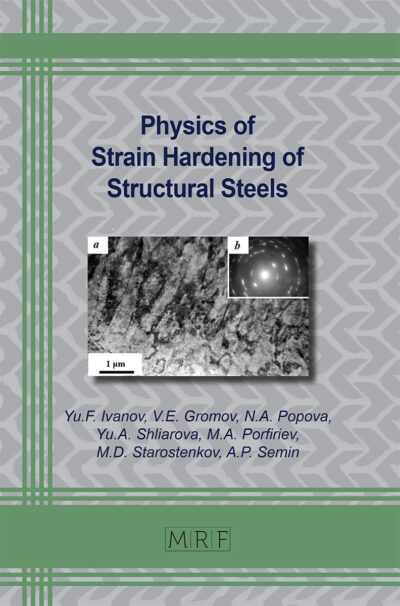
Materials: Material characterization is an ideal application area for Raman spectroscopy, due to its high chemical specificity and rapid, non-contact measurement. Solid, liquid, or gaseous, nearly all materials possess a unique Raman spectral fingerprint. The technique can be readily scaled to microscopic approaches, allowing interrogation of extremely small volumes and samples, such as nanomaterials. Characterization of nanomaterials is critical to determining structural and conformational properties. Raman spectroscopy is a highly efficient technique to study the electronic properties, compositions, and mechanical stresses in these materials, all of which can manifest in Raman band shape and frequency shift.
Semiconductor: Raman spectroscopy has proven to be one of the most effective tools for characterization of semiconductor properties and for manufacturing process/quality control because materials such as Si, SiGe, InGaAs, GaAs, GaN, and graphene exhibit precise, distinct Raman bands. Applied in a microscopic approach, the Raman technique has been successfully implemented to determine microstructure composition on thin-films, strain in the multilayer device, and to identify defects across the wafer surface.
Process/Reaction: Unlike conventional UV-Vis and NIR monitoring techniques, Raman spectroscopy provides molecular specificity in real-time measurements of gas, liquid, and solid samples, both natural and synthetic. These attributes are responsible for the emerging reliance on Raman spectroscopy for a number of online process and reaction monitoring applications. Numerous sampling options, including fiber optic probes with long reach and stand-off probes for measuring inside containers and vessels make the technique adaptable to a myriad of environments and conditions.
Surface-Enhanced Raman: Surface-enhanced Raman spectroscopy (SERS) utilizes specialized metal substrates to allow Raman signal enhancement up to 10 orders of magnitude. This phenomenon occurs when the molecules of interest are in very close proximity to the metal substrate, and is generally used for evaporated solutions or particle-surface characterization. The enhanced Raman signal with SERS has extended its applications in many fields, such as biological studies, to quantify trace substances or identify very small structures such as cell surface proteins. Intracellular SERS is also possible, via the injection of metallic nanoparticles, to study internal structures and analytes.
ElektroPhysik is one of the leading manufacturers of measuring instruments used for advancing surface technology, research and quality control. Being a pioneer in the field of non-destructive coating thickness measurement, ElektroPhysik, in cooperation with national and international standardizing institutes and universities has successfully advanced new product developments along with international standardization of the coating thickness measurement.
ElektroPhysik privately held company owned and managed by the Steingroever family. It is headquarters are in Köln Germany near the famous Rein River. ElektroPhysik still occupies the original building though it has gone through many expansions over the years to facilitate growth.
ElektroPhysik maintains branch offices including the U.S.A. and is represented by distributors and agents globally in almost every country in the world. It is this network and partnerships that enable ElektroPhysik to service its customers and provide the support required in today's competitive global marketplace.
The first coating thickness testing gauge was developed by Dr. Steingroever. Utilizing the Magnetic Attraction principle, it was called the MikroTest (still manufactured today and even available in digital display format, it probably remains the most utilized coating thickness testing device utilized, even today) . Magnetic Attraction is a very reliable technique for measuring coatings however its only drawback is that it only works with coatings applied over ferrous materials such as steel and iron.
However, the Magnetic Attraction principle paved the way for the development of analog devices. First using Eddy Current and then later Magnetic Induction, these devices expanded coating thickness testing beyond just corrosion control.
Today all three of these principles are used to non-destructively measure a variety of coatings. Magnetic Attraction is the measuring principle used in the MikroTest, PenTest and MiniPen by ElektroPhysik.
Magnetic Induction is the measuring principle of choice for ferrous metal substrate application while the Eddy Current principle is the measuring principle of choice for non-ferrous metal substrate applications.
Both of these measuring principles are found in the MiniTest family of gauges as well as the eXacto by ElektroPhysik.
More recently ElektroPhysik developed yet another measuring principle primarily for non-metal substrate applications such plastic and wood. The QuintSonic utilizes a high level ultrasound approach which has enabled measurements to be conducted on these types of substrates non-destructively.
On April 20, 2007 ElektroPhysik launched a new model, the MiniTest 700 Series with SIDSP® digital sensor technology.
SIDSP® is an ElektroPhysik exclusive which took years of research and development. SIDSP® stands for Sensor Integrated Digital Signal Processing and the way that works is that entire coating thickness measurement is processed in the sensor at the point of measurement. SIDSP® is unlike previous conventional techniques where an analog signal was generated at the sensor and then that signal would be sent to a host gauge to processing. The vulnerability with that technique was that it was susceptible to environmental influences such as strong electro-magnetic fields and other signal disturbances that could affect the analog signal and therefore the reading.
NanoFocus AG is a developer, manufacturer, and distributor of measurement technology and software packages for the characterization of technical surfaces. The company has been active in this field since 1994. Our confocal optical 3D surface analysis tools offer perfect quality assurance, process control and manufacturing efficiency for all industries and applications. NanoFocus AG's analysis systems allow high precision micro and nano scale 3D surface measurements. The innovative systems enable extremely fast, easy and contactless 3D measurements of topography, micro-geometry, roughness or other surface characteristics.
Materials Science Applications:
Optimizing functional properties if new surfaces and products:
Finding out in what way the structure of a material influences its properties and behaviour is the aim of materials science. High-resolution analyses of surfaces play an important role in determining relevant parameters like roughness, relection, tribological properties or the surface quality.
NanoFocus measurement systems guarantee analyses conform to international standards - for different measurement task and on all materials. Defined specifications are met and processes optimized. This means that costs are reduced while development times are shortened.
Non-contact 3D surface analyses independent of materials:
NanoFocus measurement systems enable the fast and reliable 3D surface analysis of nearly all materials - from metal, glass, ceramics, semi-conductors, polymers to organic materials. The confocal technology enables determining reliable measurement data independent of the degree of reflection of a surface. The optical method of the NanoFocus-technologies µsurf, µscan and µsprint also enables the non-destructive measurements of sensible surfaces at different stages of production and processing. The measurements of coated surfaces and the determination of layer thickness are also possible.
A previous sample preparation is not necessary. Real 3D data is available after only a few seconds which allows a qualitative as well as a quantitative evaluation of the surface. For the determination of relevant parameters NanoFocus offers comprehensive and powerful software solutions for the analysis of measurement data.
Examples of application:
NanoFocus measurement systems have proven themselves in many areas of materials science due their flexibility. Within only a few seconds they deliver exact and repeatable 3D measurement data of nearly all surfaces. That is why the NanoFocus-technology is ideal for user who wish to analyze different materials.
Nanoscience Instruments provides surface science, microscopy and nanotechnology solutions to customers in academia, research, and industrial markets. Our customers benefit from our products' ease of use, user-friendly interface, and low cost of ownership.
Our team of scientists and engineers have backgrounds in chemistry, biochemistry, material science, physics, and engineering. Our combined experience covers scanning probe microscopy, electron microscopy, metrology, and materials characterization techniques. Our Sales, Applications and Service teams contribute to supporting our customers and helping to solve their problems.
We partner with innovative instrumentation manufacturers across North America and Europe and provide sales, marketing, service, and application development expertise. Our portfolio includes desktop SEMs, portable AFMs & STMs, optical profilers, micro and nanomechanical testing and positioning systems. We work closely with the manufacturers' application and development teams to pair market needs with our product solutions. This approach ensures the best customer satisfaction.
Nanoscience Instruments was founded in 2002 with headquarters and an Applications lab in Phoenix, AZ. We have an Application lab and sales office in Alexandria, VA, with sales offices throughout the US.
Products:
Scanning Electron Microscopy
Atomic Force Microscopy
Scanning Tunneling Microscopy
Optical Metrology
Nanoindentation
Micromechanical Testing and Manipulation
Carbon Nanotube Synthesis
Dage was founded in 1961 and is a market leader in its chosen markets of Semiconductor and PCBA Manufacture. It has an award winning portfolio of Bondtester and X-ray Inspection Systems for destructive and non-destructive mechanical testing and inspection of electronic components.
Dage was acquired by the Nordson Corporation in 2006.
Products:
Bondtesters
Micro Materials Tester
Software
Wafer X-Ray Metrology
X-Ray Inspection Systems
Test Types include:
Shear
Brittle Fracture Testing
Compression Testing
Creep Testing
Fatigue Testing
Flexural Testing
High Strain Rate
Peel Testing
Torsion Testing
Wafer
Scientec Ibérica, subsidiary of Scientec France, whose mission is to serve and cater the Iberian market for the characterization of nano-scale surface micro from his office in Madrid.
Scientec globally specializes in the distribution of scientific equipment quality, rigorously selected, and focused on the nanoscale; providing its customers a complete solution for their metrological or experimental needs.
With over 15 years experience in Nanotechnology, our sales engineers will help you choose the most appropriate tool in your configuration, our applications group will train and help you use the selected machines, and our after-sales support service teams maintain preventive or fix your faults.
This way your investment will be guaranteed by a perfect combination of first class equipment along with the expertise, experience and knowledge of the product distribution.
Products:
Scanning probe
Optical Profilometry
Mechanical Profilometry
Nano-Indentation
Thin Films
Vacuum Technology
Ultra High Vacuum systems
Manipulators
Goniometer
Chamber
Sample holders
Instruments
Accessories
Electronics
Software
Services
Spectra Research Corporation (SRC) offers a range of innovative high-quality scientific products and laboratory services to industrial and scientific markets throughout Canada.
By selecting only the best products available and offering complete technical support, SRC is striving for continual improvement of our services and quality practices.
If you require exceptional laboratory services and support, our technical expertise and industry knowledge allows us to provide service and training for all the products we represent.
You may choose in-house or web-based training and/or technical support for all our suppliers. Tailor-made programs are also available to meet your specific circumstances. We can also put you in touch with expert application scientists who will work with you directly.
Established in 1993, SRC is a subsidiary of Allan Crawford Associates (ACA), one of Canada's largest distributors of electronic components, test equipment and integrated networking solutions.
Technologies:
Atomic Force Microscopy
Lab Scale Processing
Lasers and Photonics
Materials Characterization
Nanomechanical Testing
Particle Characterization
Rheology and Viscometry
Spectroscopy
Stability Testing
Surface Plasmon Resonance
Thermal Analysis
Vibration and Acoustic Isolation

For nearly 50 years, TREK , INC. has been providing innovative electrostatic measurement and high-voltage power solutions to customers worldwide. Trek's superior engineering design capability and manufacturing facilities allow us to provide high quality, cost-effective products and services to meet market needs and customer-specific applications.
Our proprietary technology and technical expertise, coupled with our long-term relationships, sets us apart from our competitors and has made us the leader in the markets we serve.
Trek's commitment to develop new technologies will enable us to continue to provide current and future customers with innovative solutions.
A significant portion of Trek's business is derived from the design and manufacture of custom products for OEM customers. Trek has been supplying solutions to some of these customers for over 20 years. Although we cannot disclose information about our custom OEM designs, the following provides some perspective on our capabilities. If this information interests you, please contact us to initiate a dialogue regarding your specific requirements for custom-designed product solutions.
Applications:
Electrophotography
ESD
Piezoelectronics
Research & Development
Semiconductor
Power Amplification
Metrology: These products are used for precision measurements of voltage and surface charge distributions; resistance and resistivity meters are also utilized.