4Wave is the industry leader in thin film nanotechnology material science and products. Our core technology is Ion Beam technology and Biased target technology. 4Wave offers the most advanced and cost efficient technologies for Ion Beam Etching (IBE), Ion Beam deposition sputtering (IBS) and Biased Target Sputtering BTS. 4Wave is the industry leader in the development of thin film processes and applications.
4Wave is a global company with products in North America (US and Canada), Europe and Asia. 4Wave offers products and solutions to various markets including Semiconductor, MEMS (Micro-Electromechanical Systems), Data Storage and thin film optics.
Products
Ion Beam Sputtering Cluster Tool
Laboratory Alloy and Nanolayer System (LANS)
Load Lock Etch System
Planetary Etch System (PSIBE)
Z-Flex System
Core Services
Design & Prototyping
Engineering Services
Equipment Refurbishment
Optical Thin Film Coatings
Thin Film Processing
Technology
Biased Target Sputtering (BTS)
Direct Ion Beam Deposition
In-Situ Process Monitoring
Ion Assisted Evaporation
Ion Beam Etch
Ion Beam Sputtering
A world leader in black coating services and thin film production. Our products aims to give materials and opto-mechanical parts high absorptance & high emissivity for stray light suppression in high performance optics.
We develop, industrialize and produce light absorbing Black coatings based on advanced and fast vacuum deposition technologies.
- Black coating services: Choose one of the most suitable coating services for a wide variety of substrates as metals, ceramics or polymers.
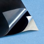
- Black foils and films: Order a tiny package of self adhesive black foils or films or get a whole roll of black coating film with outstanding optical performance.
- Blackened opto-mechanical components: Find Light traps, light trapping panels, noise reduction extension tubes, superblack precision pinholes and air slits, laser beam dumps and more.
- 3D biOptical Surfaces: Our Microtiter plates, microarray slides and transparent bottom cell culture coated microplates produced with enhanced characteristics as: Zero fluorescence background (ELISA – fluorescent detection), extremely high light absorptance, improved signal to noise ratio, controlled structural and chemical properties
AEP is the world leader in surface metrology and technology innovation. From its inception it has developed cutting edge instruments to aid researchers and users. As the pioneers of innovation in hi tech engineering, it has grown steadily in worldwide markets. Currently it has offices in America, Asia and Europe.
In addition to manufacturing optical profiler, interferometer and contact profilometer AEP also produces ex-situ and in-situ stress monitors for thin film deposition processes. Please contact us for any questions. Our team of scientists from silicon valley are always excited to answer your questions and help solve your problems.
Applications:
Step heights measurement
Surface Roughness measurement
Quantify scratch and dig features, wear depth, width and volume
Flatness or curvature measurement
2D thin film stress measurement
Film thickness
Surface Profiling - defect, features etc. depth, width and volume
Hardness
Wear Lubricity
Scratch
Roughness
Friction
Adhesion
Defectivity
Fatigue
Durability
Creep Cracks
Tensile
Stress
Indent
Delamination
Elasticity
Modulus
AJA International, Inc. was founded in Scituate, Massachusetts, USA in 1989 by William Hale, MBA, BS Physics. The company was established as a supplier of innovative thin film, vacuum and microwave products.
Prior to founding AJA International, Mr. Hale developed numerous sputter systems, ECR systems, and worked extensively in RIE, PECVD, surface analysis and vacuum technology areas ranging from chemical/pharmaceutical to vacuum packaging to UHV/MBE. This experience along with a long experience in international business gave AJA International, Inc. a solid running start.
Within 2 years the company developed the popular ATC Series Sputtering Systems - the first commercial, con-focal, sputter tools with rotating substrates and in-situ tilting magnetron sputter heads. This revolutionary development yielded extremely uniform and controllable depositions of single layers, multi-layers and alloys and has become the most popular R&D sputtering system configuration on the market.
AJA sells its products directly or in cooperation with local agents. All AJA systems are installed by AJA factory personnel whenever possible and factory acceptance and training are highly recommended and welcomed. With over 900 systems and over 7,500 magnetrons shipped worldwide, AJA International, Inc. continues to discover innovative design solutions which are often copied but never equaled as the company truly remains THE CUTTING EDGE IN THIN FILM TECHNOLOGY.
Products
Sputtering Systems
Ion Mill Systems
Evaporation Systems
Multi-Technique Systems
Sputtering Sources
Substrate Holders
Sputtering Targets
Evaporation Materials
Mark Bernick founded Angstrom Sciences, Inc. in 1988 to supply advanced magnetrons and refined materials for plasma vapor deposition of high quality thin films. With a strong focus on research and development, the company soon patented several technical advancements in magnetics, water-cooling, and circular magnetron target clamping designs.
Magnetron sputtering technology has been utilized in production applications for several decades. The basic technology used to control process plasma within the deposition process is well established within the field; however the capabilities available to optimize process efficiencies, such as thin film uniformity, target utilization, and deposition rate, are continuously evolving.
Angstrom Sciences is focused upon the development of magnetron sputtering cathodes that optimize sputter process performance. The Angstrom Advantage is the collective set of technical and structural advancements Angstrom Sciences has designed into its magnetrons in order to provide its clients with the most control over their thin film deposition process
Angstrom Sciences strives for all our customers to have complete satisfaction with our products. We offer a 2-year warranty against defects in workmanship and materials on all our magnetrons, which is the longest in the industry. We offer unlimited post-sale support to all our customers. With over 25 years of experience in the industry, we have a wealth of knowledge not only on magnetrons, but the processes they are used in. We feel it is important to share this knowledge with our customers, so that they are successful. We feel that our continued success is driven by that of our customers
We use only the highest qualtity materials, design and manufacturing techniques in order to provide the best possible product. Our in-house manufacturing capabilities along with a full-scale R&D and test lab give us the ability to fully control design development, manufacturing, and pre-shipment testing for on-time deliveries.
Products
Magnetron Technology
Magnetrons
PVD Materials
Reactive Gas Control
PVD Coating R&D
Angstrom Sun Technologies Inc. is a privately held company, headquartered in Boston, USA. The focus of company is to provide a series of cost-effective optical solutions for characterizing thin film thickness, thick coating thickness, their optical properties (refractive index N and extinction coefficient K), surface and interface behavior, alloy concentrations and their uniformities across surface.
Affordable, low cost, but advanced and high performance tools, including spectroscopic reflectometer, microspectrophotometer, microreflectometer, film thickness mapping system, simple desktop film thickness station, and automatic variable angle spectroscopic ellipsometers, offer a way to probe film stacks nondestructively and precisely. In addition, Angstrom Sun Technologies Inc. also delivers advanced analytical services for characterizing thin films, thick coatings and complicated layer stacks.
Angstrom Sun Technologies Inc. designs and manufactures all TFProbe tools in a facility located in Boston, USA. TFProbe tools are sold and distributed by international sales networks.
With performance and professional support as our mission, Angstrom has established a worldwide customer base since 2002, including well-known education institutions, government agencies and Fortune 500 companies, such as NASA Marshall Space Flight Center, National Institute of Standards and Technology, Massachusetts Institute of Technology (MIT), Seoul National University, NanoTech Center (CESTM) at SUNY, Columbia University, Hewlett-Packard Co., Lockheed Martin Co., General Electric (GE), Corning Inc., Bell Laboratories, Johnson-Johnson, Mylan Technologies, Applied Materials (AMAT), Lam Research, Samsung Advanced Institute of Technology(SAIT), and MIT Lincoln Laboratory.
Products:
Spectroscopic Reflectometers
Spectroscopic Ellipsometers
Microspectrophotometers
Thin Film Mapping Systems
Integrated In-line Metrology
TFProbe Software
Accessories
Angstrom Scientific Inc. is a distributor and manufacturer's representative, focused on providing characterization solutions to the nanotech marketplace in the Americas. Companies represented:
BioNavis:
Provides surface analysis solutions in a number of key application areas.
DEBEN:
Deben manufactures innovative accessories for SEM's and TEM's, along with a large range of in-situ tensile testing stages for use with Optical Microscopes, X-Ray CT and XRD systems.
DENSsolutions:
DENSsolution is a leading supplier of top quality sample management solutions to enable atomic resolution, dynamic in-situ electron microscopy.
Encapsulix:
Encapsulix addresses the geometric scaling of critical Atomic Layer Deposition (ALD) requirements for industrial & microelectronic devices and films. Initial process focus is in thin Al2O3, TiO2 and ZnO specifically for encapsulation and barrier coatings.
Hitachi Nanotechnology Systems Division:
Hitachi Nanotechnology Systems Division (NSD) supportscustomers with a wide range of instrumentation, including scanning electron microscopy (SEM), analytical and biological transmission electron microscopy (TEM), dedicated STEM, Focused Ion Beam (FIB), tabletop microscopes, and microanalysis sample preparation systems.
Jordan Valley:
Jordan Valley Semiconductors Ltd. provides metrology solutions for thin films based on novel, rapid, non-contacting and non-destructive X-ray technology.
Kleindiek Nanotechnik
Kleindiek Nanotechnik offers a new level of precision in manipulation, probing, and characterization of nano-materials and semiconductors
Mel-build:
Mel-Build provides a wide verity of specialized holders for Transmission Electron Microscopes.
Microtrac:
Microtrac strives to provide the materials characterization world with innovative, reliable, and repeatable particle size, particle shape, particle charge, and surface area analysis instrumentation.
XEI Scientific:
XEI Scientific, Inc.provides an effective way to gently clean scanning electron microscopes (SEMs), focused ion beams (FIBs) and other vacuum systems.
Compression Presses
Anton Paar TriTec SA (previously CSM Instruments) has been leader in the development of instruments for surface mechanical properties characterization for over 30 years in both research and industrial fields.
CSM Instruments develops, manufactures and sells instruments to characterize mechanical properties of surfaces. We have been the world leader in this market for more than 30 years, first under the name of LSRH then CSEM.
CSM Instruments provides equipment that allows the mechanical characterization of a wide range of surfaces and bulk materials. Adhesion of paints, optical thin films or hard coatings can be defined using one of our Scratch Testers. These span the nano to the macro range to analyze the widest range of materials. Dynamic testing measurements can be performed to define not only the hardness of the material, but also to evaluate the plastic and elastic deformation, the elasticity module, creep and much more. For wear testing we offer the Tribometer, based on the pin-on-disc principle that operates both in the Micro and Nano regime; to record the frictional coefficient and measure the wear volume. Other equipment measures film thickness. Additionally, CSM provides three dimensional viewing capabilities of sample surfaces under most testing regimes.
Products
Indentation Testers
Scratch Test
Tribometer
Coating Thickness by Calotest
3D Imaging
Horology
NanoMaterials Ltd. (Apnano) was established in 2002 and after its acquisition in 2013 became a fully owned subsidiary of the leading American company Nanotech Industrial Solutions, Inc. (NIS). NanoMaterials specializes in development and production of inorganic, multi-layered nanofullerenes and nanotubes, based on exclusively patented platform technology developed at the Weizmann Institute of Science.
These tungsten disulfide (WS2) based nanomaterials opened up new possibilities for developing extreme performance lubricants, coatings and polymer composites. The composition and morphology of these materials create a unique mechanism of friction-induced tribofilm release. The exfoliated nanoparticles attach to working-surfaces, fill in wear crevices and coat working surfaces with a continuous super-lubrication layer. This "surface reconditioning" effect was instrumental in the successful development of NIS's Corp, award winning NanoLub® family of Extreme Pressure (EP) Anti-Wear (AW) and Anti-Friction (AF) lubrication additives. The Company's R&D department is involved in extensive research and testing for additional WS2 based applications in the field of lubricants, coatings and polymer composites for such industries as defense, mining and metalworking.
NanoMaterials' inorganic nano-particles can be incorporated into polymer matrices to increase their strength and fracture toughness, and enhance their tribological and thermal properties.
NanoMaterials' multi-layered WS? nano-particles tackle one of the key problems of carbon nano-tubes, which is high rates of defects and agglomeration that translate to problematic dispersability.
Aremco' Equipment Division manufactures a series of high reliability equipment for the electronics, ceramics and metallurgical industries including: (1)Screen Printers for thick-film microelectronics, liquid crystal displays, brazing, and photovoltaics; and (2) Furnaces for heat treating, assaying and powder metallurgy.
Aremco's advanced material division is a leader in the development and production of technical ceramics, adhesives, coatings, sealants and potting compounds for applications to 3200 ºF. These materials are used throughout industry in the design of sensors, electrical components and analytical instruments. Industries served include automotive, aerospace, chemical processing, metallurgical, power generation and semiconductor.
Aremco's Crystalbond and Wafer-Mount adhesives are ideal materials for temporarily mounting products that require dicing, polishing, and other machining processes. These adhesives exhibit high bond strength and adhere readily to metals, glass and ceramics. When processing is complete, reheating and cleaning with one of Aremco's environmentally friendly cleaning agents removes these adhesives.

