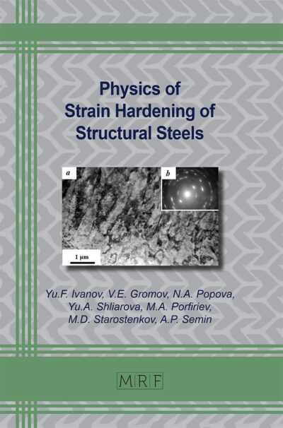
Mark Bernick founded Angstrom Sciences, Inc. in 1988 to supply advanced magnetrons and refined materials for plasma vapor deposition of high quality thin films. With a strong focus on research and development, the company soon patented several technical advancements in magnetics, water-cooling, and circular magnetron target clamping designs.
Magnetron sputtering technology has been utilized in production applications for several decades. The basic technology used to control process plasma within the deposition process is well established within the field; however the capabilities available to optimize process efficiencies, such as thin film uniformity, target utilization, and deposition rate, are continuously evolving.
Angstrom Sciences is focused upon the development of magnetron sputtering cathodes that optimize sputter process performance. The Angstrom Advantage is the collective set of technical and structural advancements Angstrom Sciences has designed into its magnetrons in order to provide its clients with the most control over their thin film deposition process
Angstrom Sciences strives for all our customers to have complete satisfaction with our products. We offer a 2-year warranty against defects in workmanship and materials on all our magnetrons, which is the longest in the industry. We offer unlimited post-sale support to all our customers. With over 25 years of experience in the industry, we have a wealth of knowledge not only on magnetrons, but the processes they are used in. We feel it is important to share this knowledge with our customers, so that they are successful. We feel that our continued success is driven by that of our customers
We use only the highest qualtity materials, design and manufacturing techniques in order to provide the best possible product. Our in-house manufacturing capabilities along with a full-scale R&D and test lab give us the ability to fully control design development, manufacturing, and pre-shipment testing for on-time deliveries.
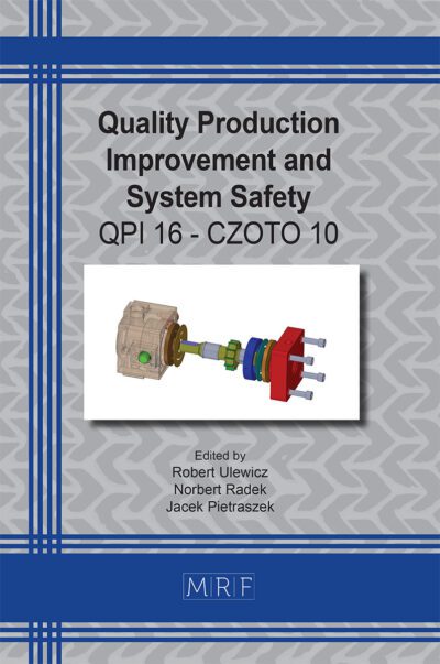
Products
Magnetron Technology
Magnetrons
PVD Materials
Reactive Gas Control
PVD Coating R&D

Founded in 2003, Arradiance® combines unique talents in material science, charged particle physics, equipment design, modeling, simulation, vacuum technology, and metrology providing world class application of Atomic Layer Deposition(ALD) and Plasma Enhanced Deposition(PEALD) to the GEMStar XT product line.
With a concentration in Atomic Layer Deposition, charged particle physics and amplification, Arradiance is the first to develop and demonstrate the capability of producing high gain, low noise, and long life micro channel amplifiers. Using Atomic Layer Deposition (ALD) materials and equipment, Arradiance offers a new approach to electron amplification devices replacing the legacy traditional lead-glass/hydrogen firing process developed in 1960's currently used for all state-of-the-art MCP applications.
Arradiance Atomic Layer Deposition (ALD) technology enables research in many areas:
MCP (Micro Channel Plate) Electron Amplification
Catalysis Systems
Medical Imaging
Space Sciences
Solar Cells
Night Vision
Alternative Energy
Thermal and Fast Neutron Detection
AXIC, Inc. was founded in 1980 as a company to develop surface science equipment for the semiconductor, electronics, and general scientific community. Initial developments focused on x-ray and electron beam analysis of surfaces for compositional and film thickness analysis. These developments lead to the introduction of a stand alone x-ray fluorescence unit which was easily operated by fab personnel for the measurement of film composition and thickness. AXIC, Inc. now produces 3 XRF systems for coatings analysis in both development and production applications for the semiconductor, magnetic, and superconductor industries.
In 1992, AXIC entered the market of producing laser based reflectometers for the measurement of film thickness, index of refraction, and film absorption properties of transparent/translucent films for the semiconductor, optical and magnetics industries.
Shortly after, AXIC commenced the manufacture of plasma tools for cleaning, photoresist stripping, reactive ion etch (RIE), and plasma enhanced chemical vapor deposition (PECVD). Today these offerings include the MultiMode HF8, PlasmaStar, and BenchMark 800-II. Units are ideally suited for research and development and small scale productions. The plasma tools can be configured in various ways to meet the end users' specific requirements.
COOKE VACUUM designs and manufactures a wide range of standard and custom high and ultrahigh vacuum systems intended for research and production. With five decades of experience, and thousands of units in the field, COOKE VACUUM has come to symbolize economy and versatility,
Cooke Vacuum Products was established in the late 1950's during an exciting period of experimentation in vacuum technology, especially thin film coating and materials research. From the beginning, Cooke had to pioneer new applications and new tools for the emerging semiconductor and optical industries, and for the related research laboratories.
Over the next decades, Cooke continued to support R&D by developing pumping systems, resistance evaporation, electron-beam, sputtering, and plasma sources, often in close collaboration with customers. Vacuum environmental chambers were developed for the space industry, encapsulation and bake systems for early flat panel displays. New, and highly specialized equipment was made for the quartz crystal industry, as well as for production of printing foil, then holographic foil. We were there to make the first OLED systems, and the first glove-box processors.
Because of the emphasis on custom solutions, the company has remained relatively small, and is well-known for its ability to "engineer on demand" more than for volume production.
Processes/Products
Thin Film Deposition: Thermal Resistance; Electron Beam; Sputter; PLD; OLED and Glove Box Systems.
Etch/Ash/Surface Treatment: Plasma Etch; Reactive Ion Etch; Surface Activation and Modification.
Test and Specials: Environmental Test; Space Simulators; Vacuum Ovens: Laser Die Attach.
Denton Vacuum transforms barriers into thin-film technology breakthroughs for customers across the globe in providing vacuum deposition systems. With operations in the United States and China, Denton engineers, designs and develops systems that precision-coat aerospace components, advanced optics, medical implants, solar cells, semiconductor devices and much more. Denton's technology portfolio includes thermal evaporation, ion beam etching, ion-beam-assisted evaporation, plasma-enhanced-chemical-vapor deposition (PECVD), and ion-beam-assisted deposition (IBAD) and e-beam evaporation and magnetron sputtering system (including reactive sputtering). Denton also provides value-added services and lifetime support that set new industry standards. Fifty years of tireless innovation have produced robust offerings ranging from high-volume production platforms to unique custom-engineered systems.
Techniques
Ion Beam Assisted Deposition
Ion Beam Deposition
Ion Beam Etchning
PECVD
PVD
Magnetron Sputtering
Reactive Beam Etch
Sputtering
Thermal Evaporation
Energetiq is a developer and manufacturer of advanced light sources that enable the manufacture and analysis of nano-scale structures and products. Used in complex scientific and engineering applications such as analytical instruments for life sciences and leading edge semiconductor manufacture, Energetiq's light products are based on new technology that generates high brightness across the spectrum, from 1nm to 1000nm and beyond, with high reliability, long operating life, and in a compact package.
Energetiq's light sources are used for: analytical spectroscopy, microscopy, and sensing in the life-sciences; lithography, metrology and photoresist development in semiconductor manufacturing; soft x-ray microscopy; and a variety of applications where synchrotron radiation and traditional arc-lamps have commonly been used.
Energetiq was founded in March 2004 by an experienced high technology development team with deep understanding of the high power plasma physics needed for high performance light products used by semiconductor equipment manufacturers, semiconductor wafer fabs, life sciences industries and the scientific research community. The expertise and experience of this team enables Energetiq to provide products with the highest levels of performance and reliability.

Harrick Plasma is a leading supplier of plasma equipment to the research community. We have been providing quality, low-cost, tabletop plasma cleaners specifically designed for use in university, government, and industrial research labs for over 30 years. Our plasma products have been cited in over 3000 publications and nearly 150 patents, and cover a wide variety of technical fields, including materials science research, microfluidics, and biomedical engineering, and cell biology studies. In addition, plasma treatment has been applied to many different materials as well as complex surface geometries, such as glass coverslips and slides, semiconductor wafers, fibers and fibrous scaffolds, metal and oxide nanoparticles, and porous membranes.
Products:
Basic Plasma Cleaner
Expanded Plasma Cleaner
High Power Expanded Plasma Cleaner
PlasmoFlo Gas Flow Mixer
Vacuum Pumps
Chambers and Sample Trays
Henniker Scientific supplies instruments, systems and technologies in the complimentary areas of;
Vacuum Techniques
Thin Film Deposition
UHV Surface Analysis
Plasma Surface Modification
Mass Spectrometry
We have more than 20 years of first hand technical and business experience with these technologies and markets throughout Europe, North America and Asia.
Our offices are located in the North West of the UK, just minutes from the M6/M62 interchange with Manchester and Liverpool International airports approximately 20 minutes in either direction.
Vacuum, Thin Film Deposition & UHV Surface Analysis:
Vacuum components, instruments and complete custom made solutions for general vacuum applications, vacuum based atomic & molecular physics and chemistry, thin film growth and UHV surface analysis.
Residual Gas Analysers:
Residual gas analysers. The lowest cost and highest specification residual gas analysers currently on the market. The range includes web-enabled residual gas analysers, analytical double and triple filter quadrupole mass spectrometers, and both high pressure and differentially pumped process residual gas analysers. Standard mass range options are 100, 200 and 300amu. Analytical range options include high resolution 1-6amu for e.g. He/D2 discrimination.
Residual Gas Analysers for Vacuum Processing:
Process Residual Gas Analysers are innovative in-situ process monitoring instruments that are fully integrated and field proven application-specific packages. The range includes the latest smart head technology delivering real-time on line analysis for vacuum diagnostics and process control in etching, thin film deposition (PVD and CVD) and plasma modification processes.
Plasma Cleaning & Plasma Treatment:
Plasma treatment equipment is used to modify the surfaces of materials such as polymers, textiles, ceramics and metals. The modification takes just minutes, is environmentally friendly and does not effect the bulk material properties in any other way. Different treatments are available to produce surface properties that are either ultra-clean, highly activated (to increase bonding properties), completely liquid-repellant or totally wettable.
Benchtop Gas Analysis:
Our range of benchtop gas analysis systems comprise purpose built mass spectrometers with application specific inlets and interfaces for on-line monitoring and analysis of gases, gas mixtures, vapours and dissolved gases in liquids. They are ideal for R&D, process monitoring and control in catalysis studies, thermogravimetric analyis (TGA coupling), membrane studies, fermentation process monitoring and thermal analysis etc.
Gas compositions can be measured over a wide dynamic range (ppt to 100%) with a wide range of sampling inlets to suit every application requirement. Versions are available with single inlet, 4, 8 or 16 way inlet.
Mass Spectrometers:
Quadrupole mass spectrometers & quadrupole mass spectrometer components. Exceptionally high performance instruments, components and systems for basic research in chemistry, physics and materials analysis.
high power, high resolution, high mass (up to 16,000 amu) triple-filter analysers
analogue and pulse ion counting
ion optics elements
combined energy filters
application specific ionizers (API/CI/EI/Membrane/Combined)
components, instruments and complete systems (for TPD/SIMS/Plasma/Molecular Beam/ MS/MS)
power supplies, quadrupole, octupole & hexapole ion guides and einzel lenses
The HORIBA Group of worldwide companies provides an extensive array of instruments and systems for applications ranging from automotive R&D, process and environmental monitoring, in-vitro medical diagnostics, semiconductor manufacturing and metrology, to a broad range of scientific R&D and QC measurements. Proven quality and trustworthy performance have established widespread confidence in the HORIBA Brand.
HORIBA International Corporation (HIC) commands successful leadership spanning North and South America with operations positioned coast-to-coast, including Canada and Brazil. HIC, financial holding company for all Americas-region entities, continues to experience active growth while implementing the sharing of corporate resources. Exemplifying a unified contribution to global environmental conservation, HORIBA continues its spirited commitment to society.
Science Applications include:
Atomic Emission Spectroscopy
Detectors-CCD, PDA, InGaAs
Gratings
Elemental Analyzers
Ellipsometers
Fluorescence Spectroscopy
Forensics
Glow Discharge
Microanalysis
Materials Characterization
Raman Microscopy
Photoluminescence
Fluorescence
Particle Characterization
Micro-XRF
Plasma Profiling TOFMS
We have a long standing commitment to quality and excellence in the high vacuum industry. Started in 1967 the company is a leader in manufacture of high vacuum equipment for thin film coating and etching.
Intlvac Thin Film's primary goal is to deliver value-added solutions that exceed the expectations of simple PVD and Ion Beam Sputter/Etch machine manufacturing and installation.
We started exporting our systems around the world in 2001, and now have equipment installed across the US, and in Canada, Malaysia, Singapore, Australia, and Israel.
Research and development play a major role in our technology's edge in the market. Our in-house development lab designs, engineers and manufactures machinery used for Physical Vapor Deposition and ion beam etching. We specialize in engineering solutions for a variety of specific results and outcomes using this process. We provide our customers with machinery needed for creating coatings including ion source and all parts needed to make it function. Additionally, we manufacture high quality PVD coatings using techniques such as Ion Assisted Thermal and Electron Beam Evaporation, Reactive and non-reactive magnetron sputtering. Diamond Like Carbon by Plasma Enhanced Vapor Deposition.
Intlvac Thin Film has become an authority for Ion Beam Etch/Sputter systems and reactive sputter systems for precision optical coatings.
Products & Services:
Thin Film Deposition Systems
Ion Beam Etch & Ion Beam Sputter Systems
Diamond-Like Carbon Systems
Optical Fiber Metalization
Thermal Vacuum & Space Simulation Systems
Ion Sources