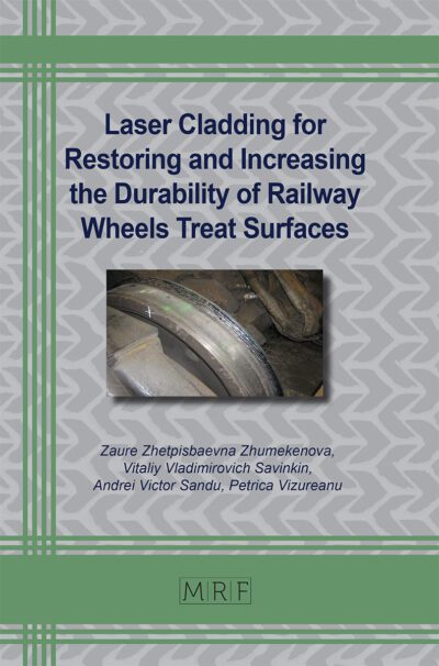
Through the employment of ultra-low temperatures, 300 Below, Inc. helps its customers improve all kinds of products by realigning the molecular structure of an object, optimally resulting in items which last significantly longer and perform far better than they were previously designed. Our proprietary process uses Deep Cryogenic Tempering, for which we have developed an advanced, computer controlled processing system for reliably treating materials used in multiple industries throughout the world. 300 Below specializes in the science of cryogenics and we engineer various liquid nitrogen (LN2) based cooling and freezing systems to perform what is termed as cryogenic processing.
As our company name implies, we treat metal components and parts at minus 300 degrees Fahrenheit to improve their properties. Computer technology allows us to regulate temperatures to 1/10th of a degree, accurately adjusting temperatures optimal for proper cryogenic treatment (or Cryo-Treatment) in accordance with the mass of the object we are treating. By reducing the temperature of an object to around -300ºF, we seek to manipulate and rearrange its molecular structure without damaging the item. By rearranging the molecular structure of an object, and realigning the molecules so that they become more uniform and evenly spread out, we then change various properties associated with the object, such as its wear resistance.
Perhaps the easiest way to understand what actually happens during the process is to picture a group of people walking around a shopping mall. We take these individuals (the molecules) and cram them into one huddled mass in the parking lot (the freezing process) and hold them there for multiple hours. We then tell this group to take one step out, one at a time, (the thawing process) so that they become equidistant from one another. Depending on the product, we may also add various stages of heat treatment using ovens that we maintain in-house to conquer various other stress factors which we seek to eliminate.
Deep Cryogenic Tempering allows for a significant increase in abrasive wear resistance and durability for many metal-based objects. There are also a few other materials which benefit from the process and we're always experimenting with companies around the globe to see if we can help improve all sorts of products. The increases we've seen in tensile strength, toughness and stability may couple with the release of internal residual stresses for different components, and some metals respond better than others. The typical end results observed by our clients include increased product life, increased durability, reduced breakage, easier cleaning abilities, and some very specific enhancements that are dependent entirely upon the project. Many changes are dependent upon the type of steel or metal used in a product, in addition to how a product was formed or created.
AEP is the world leader in surface metrology and technology innovation. From its inception it has developed cutting edge instruments to aid researchers and users. As the pioneers of innovation in hi tech engineering, it has grown steadily in worldwide markets. Currently it has offices in America, Asia and Europe.
In addition to manufacturing optical profiler, interferometer and contact profilometer AEP also produces ex-situ and in-situ stress monitors for thin film deposition processes. Please contact us for any questions. Our team of scientists from silicon valley are always excited to answer your questions and help solve your problems.
Applications:
Step heights measurement
Surface Roughness measurement
Quantify scratch and dig features, wear depth, width and volume
Flatness or curvature measurement
2D thin film stress measurement
Film thickness
Surface Profiling - defect, features etc. depth, width and volume
Hardness
Wear Lubricity
Scratch
Roughness
Friction
Adhesion
Defectivity
Fatigue
Durability
Creep Cracks
Tensile
Stress
Indent
Delamination
Elasticity
Modulus
Compression Presses
Anton Paar TriTec SA (previously CSM Instruments) has been leader in the development of instruments for surface mechanical properties characterization for over 30 years in both research and industrial fields.
CSM Instruments develops, manufactures and sells instruments to characterize mechanical properties of surfaces. We have been the world leader in this market for more than 30 years, first under the name of LSRH then CSEM.
CSM Instruments provides equipment that allows the mechanical characterization of a wide range of surfaces and bulk materials. Adhesion of paints, optical thin films or hard coatings can be defined using one of our Scratch Testers. These span the nano to the macro range to analyze the widest range of materials. Dynamic testing measurements can be performed to define not only the hardness of the material, but also to evaluate the plastic and elastic deformation, the elasticity module, creep and much more. For wear testing we offer the Tribometer, based on the pin-on-disc principle that operates both in the Micro and Nano regime; to record the frictional coefficient and measure the wear volume. Other equipment measures film thickness. Additionally, CSM provides three dimensional viewing capabilities of sample surfaces under most testing regimes.
Products
Indentation Testers
Scratch Test
Tribometer
Coating Thickness by Calotest
3D Imaging
Horology
NanoMaterials Ltd. (Apnano) was established in 2002 and after its acquisition in 2013 became a fully owned subsidiary of the leading American company Nanotech Industrial Solutions, Inc. (NIS). NanoMaterials specializes in development and production of inorganic, multi-layered nanofullerenes and nanotubes, based on exclusively patented platform technology developed at the Weizmann Institute of Science.
These tungsten disulfide (WS2) based nanomaterials opened up new possibilities for developing extreme performance lubricants, coatings and polymer composites. The composition and morphology of these materials create a unique mechanism of friction-induced tribofilm release. The exfoliated nanoparticles attach to working-surfaces, fill in wear crevices and coat working surfaces with a continuous super-lubrication layer. This "surface reconditioning" effect was instrumental in the successful development of NIS's Corp, award winning NanoLub® family of Extreme Pressure (EP) Anti-Wear (AW) and Anti-Friction (AF) lubrication additives. The Company's R&D department is involved in extensive research and testing for additional WS2 based applications in the field of lubricants, coatings and polymer composites for such industries as defense, mining and metalworking.
NanoMaterials' inorganic nano-particles can be incorporated into polymer matrices to increase their strength and fracture toughness, and enhance their tribological and thermal properties.
NanoMaterials' multi-layered WS? nano-particles tackle one of the key problems of carbon nano-tubes, which is high rates of defects and agglomeration that translate to problematic dispersability.
Fuji Electronic Industrial Co., Ltd. has taken the initiative in researches and developments of SPARK PLASMA SINTERING (SPS), PECS (Pulsed Electric Current Sintering), technology and fabricating system for leading edge High Density processing.Our results of the developments are shown widely in sintered applications for Functionally Graded Materials (FGMs), Nanophase Materials, Fine Ceramics and New Hard-metal Alloys.
Applications:
Fine ceramic materials oxides, carbides, nitrides, etc.
Functionally graded materials (FGM's): ceramic-metal, polymer-metal and other materials featuring heat resistance, hardness, electrical conductivity and grading, etc.
Electronic materials: thermoelectric semiconductors, target, magnetic and dielectric materials, etc.
Nanophase materials: Al-High-Si alloy
Hard alloy tool materials: WC/Co, ceramic or cermet cutting tools, corrosion and wear-resistant materials, etc.
Diamond tool materials: bonded cobalt and bronze segmented and straight stone grinding and cup wheels, cutting blades, etc.
Biomaterials: titanate or apatite implants, artificial bones and joints, etc.
Porous materials: ceramic and metallic bioreactors, filters, battery cell materials, etc.
Mold and die materials: press, plastic and wire drawing dies, etc.
Other sintering applications
Micro Photonics is a leading source of advanced instrumentation for scientific and industrial research. Thousands of clients rely on us for innovative solutions, technically superior products, confident application assistance, and comprehensive laboratory contract service. Since 1992 we have helped find solutions in tribology, nano-indentation, adhesion and scratch testing, profilometry, micro-tomography, imaging and other related fields of materials and thin films research.
Our instruments can be found in distinguished educational and industrial organizations ranging from automotive to cosmetic, biotechnology to medical devices, microelectronics to space applications. Regardless of your type of application, size of budget or experience in mechanical engineering research, our goal is to provide you with superior instruments, beneficial consultation and meticulous laboratory results.
Products:
Micro-CT
Graphene
Diffraction:
Nanotechnology
Surface Science
Ion Sources and Systems
MBE/UHV Components
Sources for OLEDs/Organic Electronics
Laue Diffraction Systems
Gauges:
Portable Surface Roughness Testers
Portable Hardness Testers
Digital Microscopes
Novacam Technologies Inc. designs and manufactures high-precision optical sensor systems for 3D metrology applications in industry and biomedicine. Our systems are based on low-coherence interferometry and feature fiber-based non-contact scanning probes.
Our products include:
Profilometer (profiler) systems and 3D scanners for 3D metrology, roughness measurements, thickness measurements, and cross-sectional imaging in high-precision industries
Optical coherence tomography (OCT) systems for tissue measurement and imaging in biomedicine and life sciences
Modular hardware components for original equipment manuracturers (OEMs) and for R&D
Custom metrology solutions based on low-coherence interferometry
Novacam products are used internationally in online high-technology manufacturing processes, QA/QC laboratories, R&D laboratories, and bio-medical research institutes. Clients value Novacam systems for their high precision, high speed, versatility of installation, the ability to inspect hard-to-reach surfaces and the ability to operate in hostile environments.
Novacam also partners with system integrators and OEMs who wish to incorporate Novacam advanced OCT platform components into custom assemblies for vertical markets.
Founded in 1997, Novacam is a privately held company.
Applications:
3D metrology in hard-to-reach spaces, such as inside bores, cylinders and narrow tubes;
Thickness of multi-layer or single-layer films;
Roughness, including shape, flatness and waviness;
Volume loss from surface wear; High aspect ratio features, such as steps, grooves, channels, steep slopes and holes;
Hostile environments including radioactive, very high temperature, cryogenic; Non-transparent material thickness with LIBS and profilometry
Established in 1991, Piezosystem Jena offers piezo micro positioning, piezo nano positioning and metrology solutions to the semiconductor, microscopy and synchrotron community. We have an extensive knowledge and in-depth technical expertise in the application of piezo technology to nano positioning tasks, and in the design of piezo flexure stages and development of piezomechanical systems.
Piezo based instruments are equipped with our unique piezo technology and offer XY or 3D motion with nearly unlimited resolution. Our metrology lab, with high resolution distance measuring interferometers, allows us to perform tests on custom loading configurations of piezo stages, z-axis microscopy piezo elements and piezo actuator systems with a resolution down to 50 picometers. Accurate determination of primary resonances is one of many services we can offer to our customers, ensuring that the system we provide will meet the most demanding nano positioning tasks.
Piezosystem Jena's real strength comes from our commitment to complete customer satisfaction in the markets we serve. The partnerships we form with our clientele in applications such as super resolution microscopy, AFM, process control, semiconductor metrology and nanopositioning for synchrotron radiation are long-lasting and mutually beneficial. Our knowledge in piezo technology comes as much from our interaction as consultants as it does from our own research.
Outstanding Characteristics of Piezo Elements:
Nearly unlimited resolution of the movement (sub nm)
Extemely high maximum compressive forces (multiple kN)
Movement without any mechanical play
Very short response times
No mechanical wear
Suitable for vacuum applications
Suitable for cryogenic temperatures
Piezosystem Jena develops and manufatures precision systems e.g. for the following high-tech markets:
Customized solutions to fit your special requests
More than 24 years of experience in the production and development of nanopositioning equipment
Comprehensive Consultation
Worldwide Partners, Quick Support Guaranteed
Quick Solution Propositions
Founded in 1980, SCP SCIENCE is a successful, privately owned manufacturer and distributor of analytical equipment, supplies, reagents, and certified reference materials for the inorganic analytical laboratories market. The company manufactures supply items including digestion systems, certified reference materials such as calibration and quality-control standards, and specialized glassware for the atomic spectroscopy market. In distribution, the company supplies analytical instruments for spectroscopists primarily in Canada.
Chief spectroscopic techniques supported:
Atomic absorption (AA)
Inductively coupled plasma (ICP-AES)
Inductively coupled plasma mass spectrometry (ICP-MS),
Ion chromatography (IC)
Sample preparation
Tribology
X-ray fluorescence (XRF)
Rotrode spectroscopy
Elemental analysis.
Markets served:
SCP SCIENCE supplies products to government, research and development, environment, and quality-control laboratories in the inorganic analytical spectroscopy markets. These markets include: mining, petroleum and petrochemicals, wear metals agriculture, cement, food and food processing, semiconductor, clinical, wastewater treatment facilities, and the academic and government sectors.
Taber Industries' Materials Test and Measurement Division is a global leader for the design and manufacture of high quality, affordable test instruments. Used to evaluate the physical properties of materials, Taber instruments play a critical role in the way companies test the durability of their products. Best known for our expertise in abrasion and surface wear, Taber also offers solutions to measure resistance to scratch, mar and scuff damage; along with bending resiliency and stiffness.
Products:
Wear/Abrasion
Scratch/MAR
Bending/Stiffness
Optical Micrometer